Microelectronic Systems
Microelectronic Systems
- Lecture 1
- Pin
- Lecture 2 Digital I/O
- Lecture 3 Pulse Width Modulation (PWM)
- Diode Circuits
- MOSFET(metal oxide semiconductor Field Effect Transistor)金属 - 氧化物半导体场效应管
- Lecture 6 Digital to Analogue Conversion(DAC)
- Lecture 7 Anologue to Digital Conversuib(ADC)
- Lecture 8 Numbers
- Lecture 9 Logic Gates
- Lecture 10 Multiplexer and De-multiplexer
- Lecture 11 Memory and Flip-Flops
Lecture 1
Pin
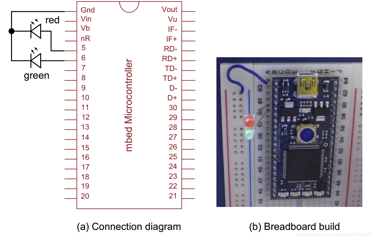
Lecture 2 Digital I/O
- to illuminate LED:
- output is high - active high
- connect to the ground V S S V_{SS} VSS(ground, negative, logic 0)
- output is low -active low
- connect to the V D D V_{DD} VDD(supply, positive, logic 1)
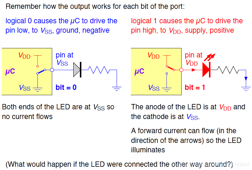
- connect to the V D D V_{DD} VDD(supply, positive, logic 1)
- output is high - active high
Lecture 3 Pulse Width Modulation (PWM)
- Duty clycle: The duty cycle is the proportion of time that the pulse is “on”, expressed as a percentage.
- simple method of using rectangulardigital waveform to control an analogue variable.
- Generating PWM : handle over specific peripheral
- Using
PwmOut:- more accurate
- Once started, the processor only needs to work if duty or period need changing
PwmOut PWM(p21);
PWM.period(4.2); // set period to be 4.2 seconds
PWM.pulsewidth(2); // set the pulsewidth to be 2 seconds
PWM.write(0.5);
//can also be simplified to
PWM=0.5; //set the duty cycle to 50%
Diode Circuits
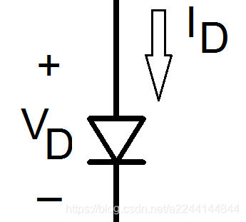
- Forward Bias
- When I D > 0 m A I_D > 0 mA ID>0mA
- V D > 0 V V_D > 0 V VD>0V
- Reverse Bias
- When I D < 0 m A I_D < 0 mA ID<0mA
- V D < 0 V V_D < 0 V VD<0V
MOSFET(metal oxide semiconductor Field Effect Transistor)金属 - 氧化物半导体场效应管
- n, p channel

| Vin | NMOS | PMOS |
|---|---|---|
| High | short(短路) | open(断开) |
| Low | open(断开) | short(短路) |
- Enhancement Mode and Depletion Mode Switches
| NMOS Enhancement Mode(增强模式) | NMOS Depletion Mode(耗尽模式) |
|---|---|
| Normally OFF | Normally ON |
| apply a voltage to make VGS more positive than the threshold voltage for an NMOSFET to turn it on | apply a voltage to make VGS more negative than the threshold voltage for an NMOSFET to turn it off |
- 2 common ways to connect or disconnect one part of circut with another
- Mechanical - physical movement is require to make or break the connection
- 如果开关在位置改变时断续接触,则可能需要使用防抖电路。
- Electrical - the conductivity of a component is changed from insulating to conducting and back again (visa versa). 组件的电导率从绝缘变为导电,然后又变回导电
- 在远程切换时很有用。 在火花可能引起火灾的危险场所中需要使用它们。电气开关的使用寿命和可靠性通常比机械开关更好。 通常,它们的尺寸小于机械开关,以允许相同量的电流流过开关。
- Mechanical - physical movement is require to make or break the connection
- 当您为mbed上的引脚分配值时,它将导致向MOSFET开关施加电压。
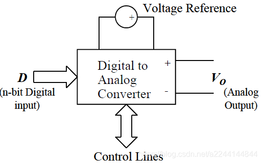
Lecture 6 Digital to Analogue Conversion(DAC)
- DAC
- numbers of possible output voltages is 2 n 2^n 2n n is the mumber of bits
- resolution is V r 2 n \frac{V_r}{2^n} 2nVr
- MAximum possible output value occurs when D m a x = ( 2 n − 1 ) D_{max}= (2^n - 1) Dmax=(2n−1)
- DAC的resolution是每个模拟值之间的步长
- conversion speed是DAC作用于输入变化的时间的倒数
- V O = D 2 n × V r V_O = \frac{D}{2^n}\times V_r VO=2nD×Vr
- Vo is the analog output voltage(模拟输出电压)
D is the value of the binary input word(二进制输入字对应的值)
n is the number of bits in the input word
Vr is the value of the voltage reference
- Vo is the analog output voltage(模拟输出电压)
/* Program to check DAC resolution of mbed*/
#include “mbed.h”
AnalogOut Aout(p18);
DigitalOut led1(LED1);
float i;
int main(){while(1){for (i=0;i<1;i=i+0.0001){Aout=i;wait(1);led1=!led1;}}
}
- total error = gain error + offset error + nonlinearity error
Lecture 7 Anologue to Digital Conversuib(ADC)
- Analog signals are converted into digital representations with a resolution and a rate determined by the Analog to Digital Converter (ADC)
- ADCs follow the ralation: D = [ f l o o r ( V i V r × 2 n ) ] B a s e 2 D=[floor(\frac{V_i}{V_r}\times 2^n)]_{Base2} D=[floor(VrVi×2n)]Base2(跟DAC是相反的)
- Note that D will never be equal to b a s e 2 ( 2 n ) base_2 (2^n) base2(2n) as the range of the ADC is limited to 2 n – 1 2^n – 1 2n–1
- V i V_i Vi is the analog input voltage
V r V_r Vr is the reference voltage
n n n is the number of bits in the converter output
- voltage comparators(12-bit ADC): N c o m p a r a t o r s = 2 n − 1 N_{comparators}=2^n-1 Ncomparators=2n−1
- output binary number is from 0 to ( 2 n – 1 ) (2^n – 1 ) (2n–1)
- 最大误差:one half of the step width;减小误差:step width should be narrowed
- Summary formulas
D = [ f l o o r ( V i V r × 2 n ) ] B a s e 2 N c o m p a r a t o r s = 2 n − 1 V s t e p = V r e f 2 n Q u a n t i s a t i o n E r r o r = V s t e p 2 D=[floor(\frac{V_i}{V_r}\times 2^n)]_{Base2}\\ N_{comparators}=2^n-1\\ V_{step}=\frac{V_{ref}}{2^n}\\ Quantisation\ Error = \frac{V_{step}}{2} D=[floor(VrVi×2n)]Base2Ncomparators=2n−1Vstep=2nVrefQuantisation Error=2Vstep - Sample and Hold
- 在执行模数转换时,对模拟信号进行“采样”并量化为ADC分辨率所定义的精度
有时,通过对几个模拟采样的结果求平均值来生成数字信号。 采样越多,只要模拟信号不发生变化,数字数据就越准确。 - 信号被保留(hold),这意味着在将信号与参考电压进行比较并生成数字信号时会暂时存储该信号
- Sampling is generally done at a fixed frequency, called the sampling frequency(通常以固定频率(称为采样频率)进行采样)
- 理想的采样频率取决于被数字化的信号的最大频率。 如果采样频率太低,则模拟信号的快速变化可能无法在结果数字数据中表示出来。
- Nyquist-Shannon采样标准规定,采样频率必须至少是最高关注频率的两倍。
- 但是,通常认为采样频率应为模拟信号中最高频率的5+倍。
- 在执行模数转换时,对模拟信号进行“采样”并量化为ADC分辨率所定义的精度
ADC/DAC Program
/*Program to explore some of the time-related aspects of the mbed DAC and ADC*/
#include "mbed.h"
AnalogOut Aout(A4);
AnalogIn Ain (A6);
DigitalOut test(D3);
float ADCdata;
int main(){while(1){ADCdata=Ain; //Perform an ADC conversiontest=1;test=0; //1 pulse on D3 shows end of the ADC conversionAout=ADCdata; //Perform a DAC conversiontest=1;test=0;test=1; //2 pulses on D3 show end of the DAC conversiontest=0;}
}
Lecture 8 Numbers
- negative binary numbers
- signed magnitude( 0 is + and 1 is -)
- one’s complement. To negate a number, replace each 1 by 0 and each 0 by 1. This holds for the sign bit as well.
- two’s complement. sign bit;
- each 1 is replaced by 0 and each 0 is replaced by 1.
- 1 is added to the result.
- excess 2 m − 1 2^{m-1} 2m−1, for m-bit numbers, represents a number by storing it as the sum of itself and 2 m − 1 2^{m-1} 2m−1
For example, for 8-bit numbers, m = 8, the system is called excess 128 and a number is stored as its true value plus 128. Thus, -3 becomes -3 + 128 = 125.
• In this case, the numbers from -128 to +127 map onto 0 to 255.
• This system is identical to two’s complement with the sign bit reversed.
- Terms
- 1 k b = 2 10 b y t e s 1 M B = 2 20 b y t e s 1 G B = 2 30 b y t e s 1 T B = 2 40 b y t e s 1\ kb = 2^{10} bytes\\1MB = 2^{20} bytes\\1GB = 2^{30}bytes\\1TB=2^{40}bytes 1 kb=210bytes1MB=220bytes1GB=230bytes1TB=240bytes
Lecture 9 Logic Gates
- Truth table
- True = logic ‘1’
- false = logic ‘0’
- Single input gates - Buffer

| A | Z |
|---|---|
| 0 | 0 |
| 1 | 1 |
- Single input gate - inverter(NOT)

| A | Z |
|---|---|
| 0 | 1 |
| 1 | 0 |
- Two input gates-and

| A | B | Z |
|---|---|---|
| 0 | 0 | 0 |
| 0 | 1 | 0 |
| 1 | 0 | 0 |
| 1 | 1 | 1 |
- Two input gates-not and

| A | B | Z |
|---|---|---|
| 0 | 0 | 1 |
| 0 | 1 | 1 |
| 1 | 0 | 1 |
| 1 | 1 | 0 |
- Two input gates-OR

| A | B | Z |
|---|---|---|
| 0 | 0 | 0 |
| 0 | 1 | 1 |
| 1 | 0 | 1 |
| 1 | 1 | 1 |
- Two Input Gates - NOR

| A | B | Z |
|---|---|---|
| 0 | 0 | 1 |
| 0 | 1 | 0 |
| 1 | 0 | 0 |
| 1 | 1 | 0 |
- Two Input Gate - XOR(Exclusive OR)
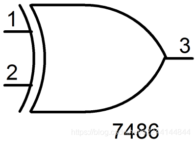
| A | B | Z |
|---|---|---|
| 0 | 0 | 0 |
| 0 | 1 | 1 |
| 1 | 0 | 1 |
| 1 | 1 | 0 |
- Boolean Expression and its Implementation
| Boolean Expression | Gate implementation |
|---|---|
| A . B A.B A.B | A AND B |
| A + B A+B A+B | A OR B |
| A ⊕ B ‾ \overline{A\oplus B} A⊕B | A XOR B |
| A ‾ \overline A A | Inverter(not A) |
| A B ‾ \overline{AB} AB | NOT(A AND B)=NAND |
| A + B ‾ \overline{A+B} A+B | NOT(A OR B) =NOR |
| A ⊕ B ‾ \overline{A\oplus B} A⊕B | NOT(A XOR B) |
-
Half Adders

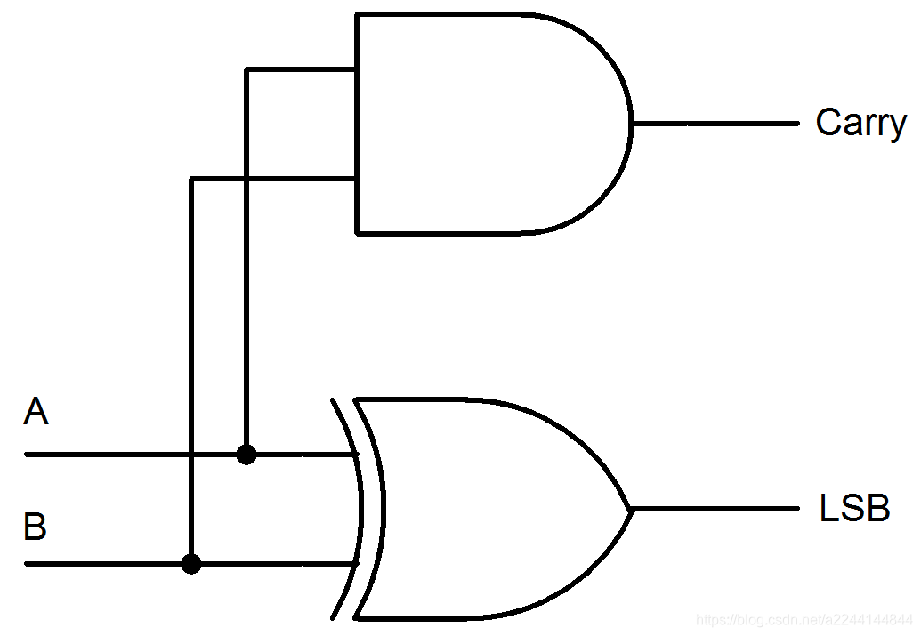
- an Excusive OR gate
- A adder with carry is an XOR gate and an AND gate.
- The output of the XOR gate is the LSB.
- The output of the AND gate is the Carry.
-
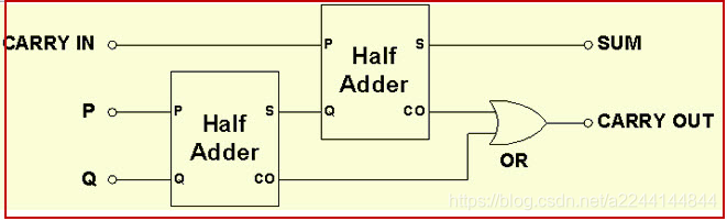
Full Adders - 3 bit adders


-
Noise Margin
- NML(noise margin low) V N L = V I L ( m a x ) − V O L ( m a x ) V_{NL} = V_{IL}(max) - V_{OL}(max) VNL=VIL(max)−VOL(max)
- NMH(noise margin high) V N H = V O H ( m i n ) − V I H ( m i n ) V_{NH} = V_{OH}(min) - V_{IH}(min) VNH=VOH(min)−VIH(min)
-
X X X – an undefined logic level that is associated with a voltage between V I L ( m a x ) V_{IL}(max) VIL(max) and V I H ( m i n ) V_{IH}(min) VIH(min).
-
Fanout
- Fanout is the maximum number of logic gates (exactly the same at then first one) that can be attached in parallel to the output of the logic gate.
-
Propagation Delay Time
- the time required for a change of voltage at the input terminals
- rise time and the fall time do not need to be the same.
- Propagation delay is the maximum delay faced by any input to reach the output.
Lecture 10 Multiplexer and De-multiplexer
- 二进制编码器,是一种多输入组合逻辑电路,可将其输入的逻辑电平“ 1”数据转换为其输出的等效二进制代码
- 多路复用器和多路分解器在许多应用中被用作减少子系统之间通信所需的导线数量的一种方式
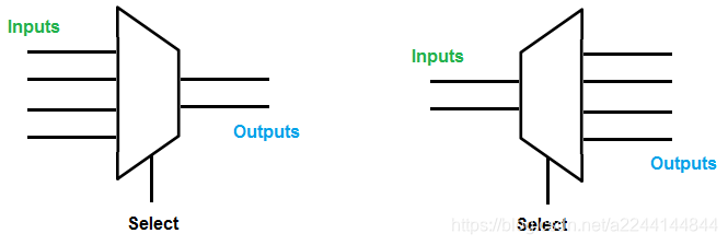
multiplexer is used ti select which of the many input signals should be transferred toits output based upon the value of an equaivalent binary number - Application
- Telephone network
- Computer memory
- Serial to parallel converter
Lecture 11 Memory and Flip-Flops
- data is held in the memory
- memory types
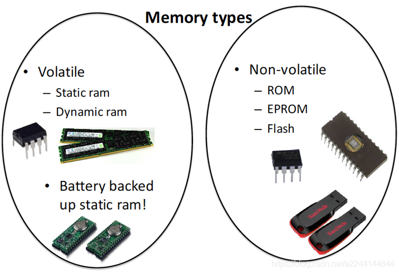
| RAM | ROM |
|---|---|
| volatile | non-volatile |
| data can be delete | permanent data |
| needs electricity, data will lose when the computer is turned off | do not need electricity, remain its data when turned off |
- Combinational logic: depend only on the state of the input
- Circuits that change the state of the output in this manner are also known as asynchronous circuits
- Sequencial logic: depend on the inputs in the past as well as present input
- Clocked circuits
- make sure to change the state at a precisely time
- change the state at the same time

- extation tables
- flip-flops cannot be simply defined by truth table.
- Control inputs
| Clear | Preset |
|---|---|
| reset the flip-flop output to 0 | set the flip-flop output to 1 |
questions:
- What is the fundamental difference between combinational and sequential logic?
- memory
- What inputs should you put on a SR flip-flop to set it (to 1)?
- 1 0;
- Why must S = R = 1 be avoided?
- 1 1 is indeterminent
- Why do sequential logic circuits need a clock?
- ensure all part of the system can change the state at the same time
- Describe the operation of a D (Data) latch. For what are they used?
- aviod 1, 1 situation of SR latch
- What is meant by the term edge-triggered flip-flop?
- respond to their inputs on either the rising or falling edge of the clock. a precise point in time rather thna an interval.
- Describe the operation of a type D flip-flop. For what are they used?
- like the chart below
| D | Q N Q_N QN | Q N + 1 Q_{N+1} QN+1 |
|---|---|---|
| 0 | 0 | 0 |
| 0 | 1 | 0 |
| 1 | 0 | 1 |
| 1 | 1 | 1 |
- Why do some flip-flops have control inputs? In what ways do they differ from the normal inputs?
- more complicated. add more functions to the circuit.
- What is the propagation delay? Why is it important?
- It limits the speed at which circuits can be clocked
- Signals that pass through different numbers of components receive different delays. Time must be allowed for all outputs to settle down before the system attempts to change state again
- The delay helps to keep digital circuits with feedback stable (this applies to virtually all practical circuits)
本文来自互联网用户投稿,文章观点仅代表作者本人,不代表本站立场,不承担相关法律责任。如若转载,请注明出处。 如若内容造成侵权/违法违规/事实不符,请点击【内容举报】进行投诉反馈!